Gate-level design
Defining operators in Scala
So far so good. We know how to build combinational logic in Scala, and have some tools available to inspect what is going on inside a circuit. And, being diligent practitioners of bottom-up design, we have immediately put our tools to use and built a small circuit that tests whether its inputs are identical.
At this point it is a good idea to pause a bit and review our programming tools.
In principle we should be satisfied with our tools. They will build us any circuit we like.
But are our tools convenient to use? Is it fun to build and play with circuits? Recall that as programmers we have the power to create our own tools, so it is not only useful but necessary to review our tools. Are our tools up to the task of building far, far more intricate combinational logic than the small circuit we just built?
Let us be critical. Look at the Scala code that builds the small circuit:
val a = new InputElement()
val b = new InputElement()
val g1 = new AndGate(a,b)
val g2 = new NotGate(a)
val g3 = new NotGate(b)
val g4 = new AndGate(g2,g3)
val out = new OrGate(g1,g4)
What we should observe immediately that it takes a lot of typing to type the code in, and the code is not particularly readable. And this is a circuit with a grand total of seven (7) gates (two of which are input elements).
At this point an experienced programmer would signal that our tools will fail us when we start scaling up our designs.
Remark. We have just observed yet another advantage of bottom-up design. If we pay attention to potential pitfalls, we can catch them early in the process. (In practice this takes quite a bit of experience with programming, but we believe it is instructive to convey how an experienced programmer thinks about a design and critically reviews the design, right from the start.)
Before proceeding further into circuit construction, let us yet sharpen our tools for increased convenience. We have just observed that we are not happy with the boilerplate that it takes to build even a small circuit, so it is a good idea to do something about this right now, before our designs have grown larger and more difficult to understand and handle.
As a first attempt to make building circuits less cumbersome,
we extend the base class Gate to get rid of the annoying
“new”-statements when building new gates. In particular, we
equip the base class with methods not, and, and or
that construct a new gate so that the current object (this) is
the (left) input to the gate being constructed, and the other
(right) input, if any, is taken as a parameter (that).
Here we go:
abstract class Gate():
  def value: Boolean     // implemented by the extending classes
  def not             = new NotGate(this)
  def and(that: Gate) = new AndGate(this, that)
  def or(that: Gate)  = new OrGate(this, that)
end Gate
This shortens our previous circuit-building code to:
val a = new InputElement()
val b = new InputElement()
val g1 = a.and(b)
val g2 = a.not
val g3 = b.not
val g4 = g2.and(g3)
val out = g1.or(g4)
Or what is the same, but avoiding the intermediate values:
val a = new InputElement()
val b = new InputElement()
val out = (a.and(b)).or(a.not.and(b.not))
The code for building the circuit is now short, but it still lacks readability. For example, think about a simple mathematical expression such as
x+y*(z-w)
and contrast this with writing the same expression as
x.plus(y.times(z.minus(w)))
Clearly the former expression is both easier to read and easier to write.
Mathematical operations of various types are frequently encountered in programming,
and hence many programming languages, Scala included, make it possible for a
programmer to define the meaning of operators such as +, -, *, and /
when they are applied to programmer-defined objects.
In our case, we are interested in building new gates by applying a logical operator
(NOT, AND, or OR) to one or two objects of type Gate. We can do this in Scala by
defining the meaning of the corresponding Boolean operators !, &&, and ||
when they are applied to objects of type Gate. Operators that act on objects
in a class are defined in Scala by defining methods with names
unary_!, &&, and || inside class Gate
(compare this with methods not, and, and or defined above):
abstract class Gate():
  def value: Boolean     // implemented by the extending classes
  def unary_!: Gate        = new NotGate(this)
  def &&(that: Gate): Gate = new AndGate(this, that)
  def ||(that: Gate): Gate = new OrGate(this, that)
end Gate
To build circuits, it now suffices to write expressions with Boolean operators
and objects of type Gate, and the resulting method calls will construct
the circuit for us. This makes it very convenient to build circuits in
Scala. That is, we build a circuit using precisely the same convenient syntax
as if we were evaluating a Boolean expression.
For example, our code for building exactly the same circuit as before now reads:
val a = new InputElement()
val b = new InputElement()
val out = (a && b) || (!a && !b)
The last line is just a syntactic shorthand for the following method calls
in class Gate:
val out = (a.&&(b)).||(a.unary_!.&&(b.unary_!))
In fact, all operator expressions in Scala are just such shorthand for method
calls. For example, a+b is a shorthand for a.+(b).
One has to be careful with precedence though, for example,
a+b*c is a shorthand for a.+(b.*(c)), not (a.+(b)).*(c).
Remark 1. Before proceeding further, let us yet again reflect where we are and what we have done. We observed that we may be facing trouble unless we make it more convenient to build circuits, and with some effort we were able to improve our circuit-building tools. Experienced programmers are constantly engaging in such dialogue with colleagues and themselves with the aim to evaluate the convenience of a design and potential pitfalls that may arise when the tools are deployed in production.
Remark 2. (**) In case you are interested in the details of how expressions are constructed in Scala from operands and operators, you may want to study Section 6.12 (“Prefix, Infix, and Postfix Operations”) in the Scala Language Specification.
Our first design – the half adder
With our circuit-building and tinkering tools sharpened, let us continue towards our goal. To arrive at a circuit that adds two 64-bit integers, it would appear like a good first step to design a circuit that adds two 1-bit integers. We know how to add 1-bit integers, in binary:
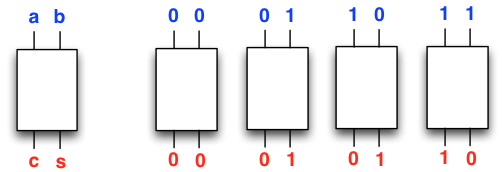
It looks like we need to have a 2-bit output from our circuit, because \(1 + 1\) in binary produces the carry \(1 + 1 = 10\). So our specification reads:
Or in circuit terms, we need a circuit that takes two inputs, and produces two outputs, with the following specification:
Here is a circuit that meets the specification (check this!):
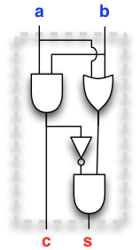
Or what is the same, in Scala (check this with Toggler):
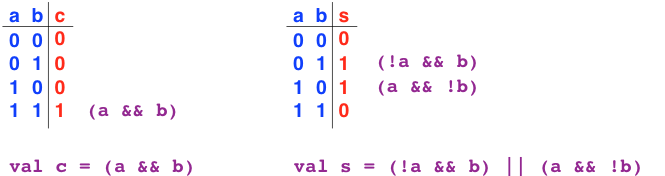
val a = new InputElement()
val b = new InputElement()
val c = a && b
val s = (a || b) && !c
But hold on! How did we actually come up with the circuit?
How does one design circuits that meet a specification?
Specification and implementation – the truth table and synthesis
One way to specify what a circuit needs to do is to list what must happen at the output (or at each output, if there are multiple outputs) for every possible input to the circuit. Such a specification is called a truth table.
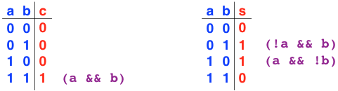
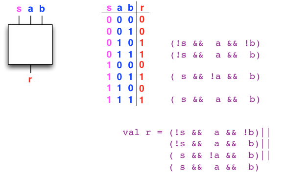
Here is a truth table that completely specifies a half adder:
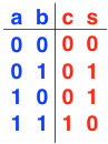
There are two inputs, namely the summands a and b, and two outputs, namely the sum s and the carry c.
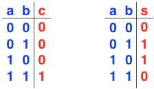
If we are dogmatic about our terminology, a truth table must specify exactly one output, so we actually have two truth tables to specify the half adder, one for each output:
A specification in general tells us in precise, unequivocal terms what must be done. For example, a specification could read as:
“The square root of a non-negative real number \(x\) is a non-negative real number \(y\) such that \(x = y^{2}\). Given a rational number \(x\) as input, determine a rational number that differs in absolute value from the square root of \(x\) by at most \(10^{-100}\).”
In our case, a specification tells us what the circuit must do. A truth table gives a precise specification for (one output of) a circuit.
An implementation in general tells us in precise, unequivocal terms how to do it, or, depending on perspective, “actually does it”. For example, square roots may be computed to an arbitrary precision using Newton’s method.
So how does one implement (or synthesize) a circuit from a truth table?
One possible strategy is to simply
“read the 1-output rows” in a table.
Namely, for each 1-output row,
we write an AND-expression of inputs
(or NOT-ted inputs) such that the AND-expression is true
exactly when the inputs match the values given in the row.
Let us do this for both of our truth tables, one 1-output row at a time:
Next, we simply take the OR of the expressions that we have written. We now have an implementation of the specification.
Or what is the same, drawn as a circuit:
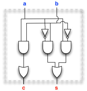
Circuits constructed in this form are called OR-AND circuits because of their “outer” (closer to outputs) layer of OR-gates and “inner” (closer to inputs) layer of AND-gates. Alternatively, OR-AND circuits are said to be in disjunctive normal form or DNF.
Remark. Again it is a good idea to pause and reflect what we have just learned. As soon as we know what we want (or more precisely, as soon as we can write a truth table), we also know how to get it. That is, we know how to build a machine (a Boolean circuit) that does what we want. We simply synthesize the circuit from the truth table.
Configurability – data and control
Let us now put our new skills at specification and implementation into action. In particular, since we now know how to build machines that do what we want, it is more than appropriate to make a first attack at resolving the mystery of programmability. How do we build machines that are programmable and will do whatever we instruct them to do?
Programming is about control. We have the power (instrumented by a programming language) to tell the machine what to do. But how is this power available and implemented, built into the machine? What is the origin of the versatility that we witness in a computer?
Again let us think about this by starting from the bottom up.
What is control? Simplified to the extreme, and thinking in Boolean terms, perhaps an ON/OFF switch would be a good starting point.
A switch – say, a light switch – is a clear instrument of control.
So how would an ON/OFF switch manifest itself in Boolean circuitry?
Perhaps all that is required is a simple but fundamental change in how we view a Boolean circuit. Indeed, if we want, we can view each one-bit input to a circuit as a switch. In the simplest case, there is one input (“the switch”) that controls what the circuit does with the rest of the inputs.
Let us explore this change of view in the small. Consider a circuit that consists of a single AND-gate, and designate one of the two inputs as “the switch” s:
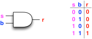
Studying the truth table from our newly adopted viewpoint, we
see that when “the switch” s
is set to false, the output r
stays at false no matter what the value of the other
input to the AND gate. When “the switch” s
is set to true, the AND gate simply passes the other input
b as is to its output r.
Already this appears like a property that we could put into good use.
So let us get more ambitious. Could we make a circuit that selects between two inputs, based on what “the switch” (a third input) says?
Of course we can. Simply write out the truth table and synthesize the circuit:
By studying the truth table, we observe that the design indeed
performs as intended. If the switch s
is set to false, the output r
equals the input a.
If the switch s is set to true,
the output r equals the input
b.
Just to be sure that this is the case, let us witness the circuit operate in Toggler:
val s = new InputElement()
val a = new InputElement()
val b = new InputElement()
val r = (!s &&  a && !b)||(!s &&  a &&  b)||( s && !a &&  b)||( s &&  a &&  b)

val t = new Toggler()
t.watch("s", s)
t.watch("a", a)
t.watch("b", b)
t.watch("r", r)
t.go()
After a minute or two of fun with Toggler, we should be convinced
that the switch s indeed selects between the inputs a and b,
just as we designed. Incidentally, an equivalent and more succinct design is:
val r = (a && !s) || (b && s)
Let us now step back and reflect a little. At this point it would appear that Boolean circuits have suddenly become more powerful, since we can now control what a circuit does. Of course this is not strictly speaking true, since the only thing that changed was our view of Boolean circuits. From a design perspective, it is useful to view that some of the inputs to a circuit are data inputs and some of the inputs are control inputs that affect how the circuit operates on the data inputs to produce the outputs. A different way of saying the same thing is that the control inputs configure the circuit.
So, in terms of the big picture, are we done yet? Is configurability the same as programmability?
No, not really. The computer is more than combinational logic.
But we are getting closer to understanding the computer. (Indeed, take a peek at programmable logic!)
Efficiency – circuit depth and size (*)
Let us conclude this section on gate-level design by briefly thinking about what constitutes an efficient circuit design for a task. Indeed, whenever we have succeeded in producing at least one design that performs a task, from an engineering perspective a key question is whether a more efficient design exists.
So what properties of a combinational circuit measure its efficiency?
If we think about a physical implementation of a circuit, numerous possibilities present themselves, ranging from power consumption to speed. In our case, however, we have chosen to abstract away physical details from our Scala circuit simulation, so physical properties are not available to enable comparison of designs.
Yet, our circuits have two properties that we can use to compare designs, and these properties are natural measures of efficiency also in the context of physical design. These two properties are circuit depth and circuit size. In physical terms, the first property measures, roughly, how fast we can run the circuit, and the second measures, again roughly, the resources required to successfully manufacture the circuit and, very roughly, its power consumption when it is operated.
Circuit depth. Physical circuits are physical objects that require time to operate. It takes time for electric signals to propagate in conductors, and it takes time for gates to stabilize their output value once their input value(s) are stable. A rough measure of the speed at which we can run a circuit is its depth, that is, the length of the longest sequence of gates whose values need to stabilize when we change the values of the input elements.
In more precise terms, the depth of a gate is defined inductively as follows. The input elements to the circuit have depth zero. The depth of a logic gate is the maximum of the depths of its input gates, plus one. The depth of a circuit is the maximum of the depths of all of its gates.
The smaller the depth, the faster we can operate a circuit. Thus, among multiple possible designs for a task, we should prefer circuits that have small depth if we desire a fast circuit.
Example.
Suppose we need to take the logical AND of 8 input elements. That is, we require
a circuit that has one output that evaluates to true if and only if each
of its 8 input elements evaluates to true. It is immediate that such
a circuit can be implemented with two-input AND-gates, and a little
reflection shows that exactly 7 two-input AND-gates are both necessary
and sufficient. But there are many ways to connect the 7 gates with each
other and the input elements. Here are two possibilities:
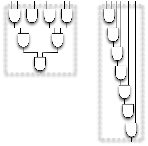
The circuit on the left has depth 3, the circuit on the right has depth 7. Clearly the circuit on the left is more efficient in terms of the depth. Many more possibilities exist beyond the two displayed circuits, but the circuit on the left is in fact the circuit with the minimum depth for the task. (What if we had 16 inputs? Or 1048576 inputs?)
Circuit size. Physical circuits are physical objects that require energy to operate and material to manufacture the circuits. Very roughly, the more gates the circuit has, the more energy and materials it requires, assuming each individual gate requires a fixed amount of both. Furthermore, a large number of gates means also increased complexity and e.g. increased probability of defects in the manufacturing process compared with a smaller design. Thus, among multiple possible designs for a task, we should prefer circuits that use the least amount of gates if we aim for low resource consumption.
To adopt a precise definition for purposes of our simulated circuits, let us define the size of a circuit to be the total number of gates in the circuit, including both logic gates and input elements.
Example. Let us revisit two of the half-adder designs that we built above. The first design has 2 inputs and 4 logic gates, so its size is 6:
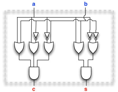
The second design has 2 inputs and 11 logic gates, so its size is 13:
Both circuits implement the half-adder, but clearly the first one is more efficient in terms of circuit size.