The armlet data path
The armlet architecture overview
Let us now start developing the armlet architecture. To enable
gate-by-gate construction using minilog, we will keep the design small.
While most modern designs have a 32- or 64-bit word length,
the armlet will have a 16-bit word length. That is, all
arithmetic and other operations on data are carried out in basic units
of 16 bits.
The architecture consists of two subsystems. Namely the
armlet processor itself, and a memory module for storing data.
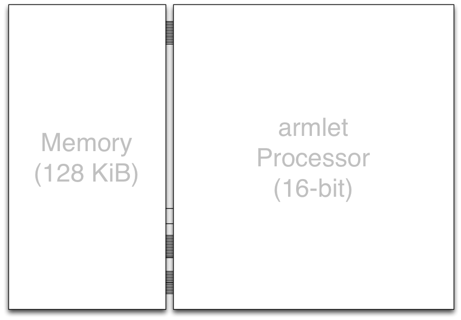
Here our focus will be on developing the processor design. The exercises will investigate how to build a memory unit in sequential logic.
In essence, the armlet processor will consist of
internal state elements (the registers),
the external interface (inputs and outputs to units external to the processor, in particular the memory unit), and
the combinational logic joining the state elements (with feedback) and the external interface.
We will develop the armlet processor in multiple
stages, at each stage making further additions to the design.
To give a quick birds-eye view to the entire architecture, here
is a diagram of the armlet at the level of subunits:
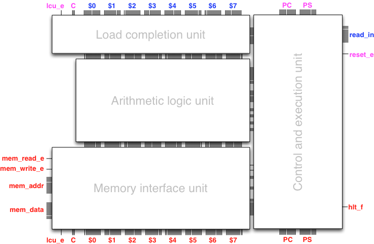
The feedbacks occur from the outputs at the bottom to matching inputs at the top in the diagram. The inputs and outputs on both sides (left and right) of the diagram are the external interface of the processor, which includes the interface to the memory module.
Our first objective will be to build the computational heart of the processor, namely the arithmetic logic unit (ALU), without paying attention to external interfaces or programmability beyond a single step (clock tick) of computation. Once the ALU is ready, we will extend the design with a simple load/store interface between registers and memory.
The armlet is fully designed, built, and simulated
in gate-level sequential logic, using package minilog.
This is convenient from a pedagogical perspective in two respects.
First, nothing is hidden. The entire processor design is about
500 lines of Scala code, and can be found in package armlet.
We can load any part or all of the design to Trigger and play
with it. (Indeed, our plan is to introduce the design first by play and
then by work, through programming the armlet.)
Caveat. The armlet is a substantially
simplified design compared with an actual ARM architecture,
whereby our main motivation and ambition is to investigate the
principles underlying a computer architecture from
a programmer’s perspective, while avoiding all details and
complexities of a physical implementation, including related
design considerations such as
pipelining, or
parallelism-enabling designs such as
multicore
or
multithreading.
With this motivation in mind, in fact only the basic
Von Neumann architecture remains,
together with a reduced instruction set that is sufficient to run
user code that interfaces with memory. Also the memory interface
is substantially simplified without e.g. caching or virtualization.
In general, processor microarchitecture
is a rapidly evolving topic requiring
substantial further study beyond the basic principles covered in
the armlet design.
Registers and processor state
The internal state of a processor resides mostly in its registers. Each register typically holds one word of state.
The armlet has 8 general-purpose registers, which
we will somewhat unimaginatively name as $0, $1,
$2, $3, $4, $5, $6,
and $7. Each register has 16 bits of state.
One may view each general-purpose register as a “variable that is physically built into the processor”.
In addition to the general-purpose registers, there are two special registers, the program counter and the processor status register, and some further state elements relevant from the perspective of control and program execution. These will be discussed and implemented into the design in Round 5: A programmable computer.
The arithmetic logic unit (ALU), first version
We now start building the combinational logic of the processor, one subunit at a time, and in multiple versions to increase the complexity of the design gradually, taking sufficient time to play to familiarize ourselves with the design.
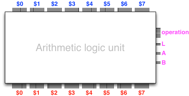
From a user perspective, the arithmetic logic unit is the part of the processor that actually takes care of the computing, one elementary operation at a time.
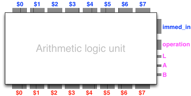
The arithmetic logic unit is a combinational circuit that takes as data input the current values of all the 8 registers (depicted at the top in the diagram below), carries out an arithmetic or logic operation that is configured via control inputs (depicted on the right), and outputs the values of all the registers after the operation has been carried out.
In general an operation affects at most one register. The outputs are then given as input to further functional units along the processor data path, and eventually fed back to the input elements when the clock triggers.
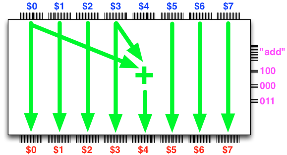
For example, one possible operation of the ALU is to
“store into the register
$4the sum of registers$0and$3”,
or what is the same in slightly more succinct form,
add $4, $0, $3
The control inputs configure the ALU to effect the desired
operation so that the inputs are transformed into the desired
output. For example, if we configure add $4, $0, $3 via
the control inputs (depicted on the right), then the ALU will
indeed effect the configured operation:
The armlet ALU supports the following eleven different
operations, which can be viewed as a reduced set of
the operations that an actual ARM processor supports:
nop                   # no operation
mov $L, $A            # $L = $A (copy the value of $A to $L)
and $L, $A, $B        # $L = bitwise AND of $A and $B
ior $L, $A, $B        # $L = bitwise (inclusive) OR of $A and $B
eor $L, $A, $B        # $L = bitwise exclusive-OR of $A and $B
not $L, $A            # $L = bitwise NOT of $A
add $L, $A, $B        # $L = $A + $B
sub $L, $A, $B        # $L = $A - $B
neg $L, $A            # $L = -$A
lsl $L, $A, $B        # $L = $A shifted to the left by $B bits
lsr $L, $A, $B        # $L = $A shifted to the right by $B bits
asr $L, $A, $B        # $L = $A (arithmetically) shifted to the right by $B bits
By convention, each operation is associated with a three-letter
mnemonic such as “add” or “ior” whose meaning is explained
on the right in the table above. The parameters “$L”, “$A”,
and “$B” each may be an arbitrary register among the registers
$0, $1, $2, $3, $4, $5, $6,
and $7.
Now all that is needed is the combinational logic to implement these
operations, with control inputs designating what operation is to be
carried out, what register(s) are used as operands ($A and $B),
and what register will receive the result ($L), if any.
If you were diligently solving the circuit-design exercises in Round 3: Combinational logic, this is where your work pays off. In fact, you have all the building blocks sufficient to build the ALU. The design of the ALU just amounts to combining these building blocks appropriately and making design decisions how to structure the control inputs to configure the ALU to compute what we want with data on the registers.
Extending the ALU – loading immediate data
The first version of our ALU already offers a fair selection of different operations and versatility in register selection, but it is lacking in one aspect. Namely, how does one load input to the registers? (Remember, the registers are inside the processor – in practice we must have some mechanism for loading data into the processor to start computing with the data.)
It would appear like a good idea to have such data-loading functionality
via an immediate data input to the ALU, whose use is configured via
the control lines. Observe the immediate data input immed_in in
the following diagram:
We extend the specification of the ALU with the following operations that accept immediate data:
mov $L, I             # $L = I (copy the immediate data I to $L)
add $L, $A, I         # $L = $A + I
sub $L, $A, I         # $L = $A - I
and $L, $A, I         # $L = bitwise AND of $A and I
ior $L, $A, I         # $L = bitwise (inclusive) OR of $A and I
eor $L, $A, I         # $L = bitwise exclusive OR of $A and I
lsl $L, $A, I         # $L = $A shifted to the left by I bits
lsr $L, $A, I         # $L = $A shifted to the right by I bits
asr $L, $A, I         # $L = $A (arithmetically) shifted to the right by I bits
So far so good. We have now specified what we want the ALU to do.
If you look at the armlet source code, the actual ALU in the final
processor design is somewhat more intricate in its inputs and outputs,
but the present specification is sufficient to start playing with the design,
which is what we will do right now.
Trigger time with the ALU
To play with the ALU circuit compile and run the file launchALUTrigger.scala in the armlet source code, or copy and paste the following to an armlet-aware console:
import armlet.*
new ALUTrigger()
A Trigger window should pop up, with a view to the ALU
circuit, and with feedbacks built from the output to the input
elements. In particular, the Trigger view displays
only the register inputs and the control inputs to configure
the operation of the ALU. This is best illustrated by a few examples
that we will review below.
The register inputs to the ALU are open to toggling, so we can toggle in some numbers. So let us toggle in some numbers to the registers:
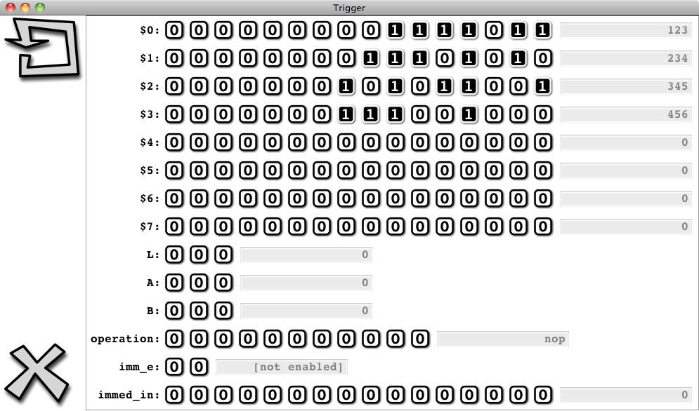
(Observe in the figure above that on the right there are convenience text
fields that decode the watched bus in decimal, or in symbolic form.
This is a convenience feature of Trigger for manipulating a watched
data bus, not part of the processor design.)
We can now configure the operation of the ALU via the control inputs.
Let us set up the operation “add $4, $0, $3”:

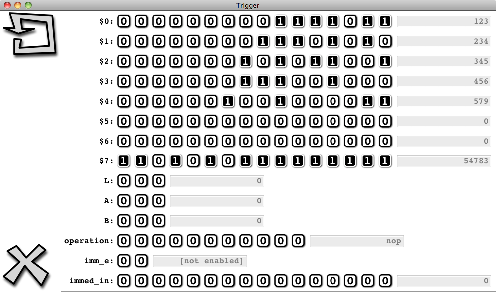
Click on the clock button to execute the operation:

The outputs feed back to the inputs, and we observe that the
ALU indeed performs precisely as instructed –
the sum of $0 and $3 appears in $4.
Next, let us set up the operation “mov $7, 54783”:

After the clock is triggered, $7 has the immediate data:
Now you are free to play with and configure the ALU as you like. All the operations specified above are available – just play with the control inputs to configure the operation, and trigger the clock to execute it. Say, playing with the shift operations can be a mesmerizing experience. Alternate between, say,
lsl $0, $0, 1
and
lsr $0, $0, 1
to witness the bits in $0 walk left and right.
What we should take home from playing with the ALU is that it is just a piece of sequential logic, conceptually not much more complex than the simple accumulator-adder that we built at the start of this round.
The ALU in Scala (**)
The ALU may look like a formidable logic design in Trigger, at
the level of Scala code the design is far less intimidating. The following
is essentially the complete code it takes to build the combinational logic
in the ALU, assuming builders for subunits such as adders and subtractors
are available as subroutines. (Note however, that the actual ALU design
in package armlet has some further functionality required by material
that we will cover in Round 5: A programmable computer.)
// A helper table of the arithmetic-and-logic operations and their
// operator-builder functions:

val ops_ALU = immutable.ArraySeq(
    ("mov" , (a: Bus, b: Bus) => a),
    ("and" , (a: Bus, b: Bus) => a & b),
    ("ior" , (a: Bus, b: Bus) => a | b),
    ("eor" , (a: Bus, b: Bus) => a ^ b),
    ("not" , (a: Bus, b: Bus) => ~a),
    ("neg" , (a: Bus, b: Bus) => buildNeg(a)),
    ("add" , (a: Bus, b: Bus) => buildAdd(a,b)),
    ("sub" , (a: Bus, b: Bus) => buildSub(a,b)),
    ("lsl" , (a: Bus, b: Bus) => buildLeftS(a,b)),
    ("lsr" , (a: Bus, b: Bus) => buildRightS(a,b)),
    ("asr" , (a: Bus, b: Bus) => buildARightS(a,b)))

// Load completion unit

def buildLCU(reg_in:     Seq[Bus],
             read_in:    Bus,
             prev_l_idx: Bus,
             lcu_e:      Gate) =

  // Complete load if load enabled

  val l_select = buildDecoder(prev_l_idx) && lcu_e
  val reg_out = (reg_in zip
                 l_select).map(x => ((x._1 && !x._2)|(read_in && x._2)))

  reg_out
end buildLCU

// Arithmetic logic unit

def buildALU(reg_in:    Seq[Bus],
             l_idx:     Bus,
             a_idx:     Bus,
             b_idx:     Bus,
             immed_in:  Bus,
             imm_a_e:   Gate,
             imm_b_e:   Gate,
             opers:     Seq[(Gate,(Bus,Bus)=>Bus)],
             reset_e:   Gate) =

  // Decode and select $A
  val a_select = buildDecoder(a_idx)
  var ra = buildBusSelector(reg_in, a_select)

  // Decode and select $B
  val b_select = buildDecoder(b_idx)
  var rb = buildBusSelector(reg_in, b_select)

  // Left operand -- register or immediate?
  val opa = (ra && !imm_a_e) | (immed_in && imm_a_e)

  // Right operand -- register or immediate?
  val opb = (rb && !imm_b_e) | (immed_in && imm_b_e)

  // Run the operation builder function for each operation
  val results = opers.map(_._2(opa,opb))

  // Comparison of operands
  val cmp_sgn = buildSub(opa,opb)
  val f_eq    = !(opa ^ opb).reduceLeft(_ || _)     // opA == opB
  val f_ab    = buildAB(opa,opb)                    // opA > opB  (unsigned)
  val f_gt    = !f_eq && !cmp_sgn(cmp_sgn.length-1) // opA > opB  (signed)

  // Select result-of-operation based on enable-signals for each operation
  val res = (results zip
             opers.map(_._1)).map(x => x._1 && x._2).reduceLeft(_ | _)

  // Save result to register if there is an operation that is enabled
  val save_e = opers.map(_._1).reduceLeft(_ || _)
  val l_select = buildDecoder(l_idx) && save_e

  val reg_save = (reg_in zip
                  l_select).map(x => ((x._1 && !x._2)|(res && x._2)))

  // Zap all regs on reset
  val reg_out = reg_save.map(_ && !reset_e)

  // Output new values of registers & flags
  (reg_out,
   f_eq,f_ab,f_gt,
   opa)
end buildALU
This is essentially all it takes to build the combinational logic in the ALU.
The Trigger interface in object ALUTrigger requires
a few more lines of code that is available in package armlet.
Now that we have reviewed the basic functionality of the arithmetic logic unit and presented its implementation, our next task is to extend the data path (which so far consists only of the arithmetic logic unit) with an interface to a memory unit. This is achieved by two subunits that occur before and after the ALU.
Memory and the armlet (*)
A processor in most cases works with a lot more data than can be stored in the processor registers. This data must be made available to the processor by interfacing the processor with dedicated storage units (memory) that hold the data.
The armlet is a load/store architecture, which means
that data must be loaded from memory to a register, and stored from
a register to memory, using dedicated operations. These operations are
implemented in the memory interface unit in the data path. But before
designing the unit, let us specify the interface that the unit uses
to access memory.
The armlet architecture has a 16-bit word length, and accordingly it
can interface with up to \(2^{16} = 65536\) words of memory that reside
in a memory unit outside the processor. Each such word consists of 16 bits,
for a total of 128 kibibytes of main memory.
Each word in the memory unit has a unique address in the range \(0,1,\ldots,65535\) by which it can be identified and its contents manipulated.
The memory unit supports two basic operations: memory read and memory write. The memory unit has the following interface:
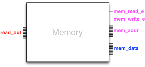
Read. A memory read is issued to the memory unit by giving
true value to mem_read_e and giving the address
of the word that is to be read as value to the bus mem_addr.
The result of the read appears in the output bus read_out
of the memory unit. This bus is then fed back from the memory unit
to the processor so that when the clock triggers,
the result of the read appears at the processor input
bus read_in.
Write. A memory write is issued to the memory unit by giving
true value to mem_write_e and giving the address
of the word that is to be written as value to the bus mem_addr.
The data that is to be written is given as value to the bus
mem_data of the memory unit.
When the clock triggers, the contents of the memory
word at this address are updated with the given data.
Caveats. Our armlet simulation considerably simplifies
an actual processor–memory interface. An actual (main) memory
unit is considerably slower than the processor in terms of the
clock speed. This is compensated in practice with
(a) one or more levels of cache memory that has less storage capacity
than main memory, but operates faster and carries
several words of data in one data block (cache line), and
(b) a high-bandwidth interface to the main memory utilizing
increased data rates and/or
multiple channels.
Memory interface unit
Let us now design the part of the armlet processor that is
responsible for interacting and interfacing with the memory unit.
The memory interface unit uses the registers and its own
control input to issue operations (read or write) to the memory unit.
Our design situates the memory interface unit immediately after the arithmetic logic unit in the data path of the processor. That is, the register inputs of the memory interface unit are the register outputs of the arithmetic logic unit:

The memory interface unit implements two operations, load from memory and store to memory:
loa $L, $A            # $L = [contents of memory word at address $A]
sto $L, $A            # [contents of memory word at address $L] = $A
The load completion unit (*)
In addition to the memory interface unit, the armlet design
has a unit that takes care of completing a load operation from memory,
that is, actually storing the data that arrives from the memory unit
into the designated register that is to receive the data. The load
completion unit occurs before the arithmetic logic unit on the
data path. That is, the load completion unit receives
its register inputs from the actual input elements (flip-flops or latches),
and gives its register outputs as input to the arithmetic logic unit.
In this way the result of a memory read issued in the previous clock
cycle gets stored in the designated register before the ALU operates
on the register in the current clock cycle.
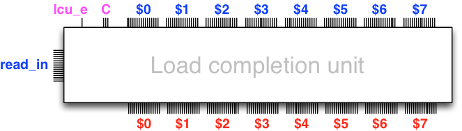
The memory interface unit is responsible for controlling the load
completion unit via the enable signal lcu_e and the
index C of the register that is to receive the data
from the memory read, which arrives via the input bus read_in.
Summary
The sequence of the load completion unit, the arithmetic logic unit,
and the memory interface unit constitute the data path
of the armlet processor. That is, the sequential logic
that evolves the state of the registers and memory based on control inputs.
We can summarize the structure of the data path with the following diagram:
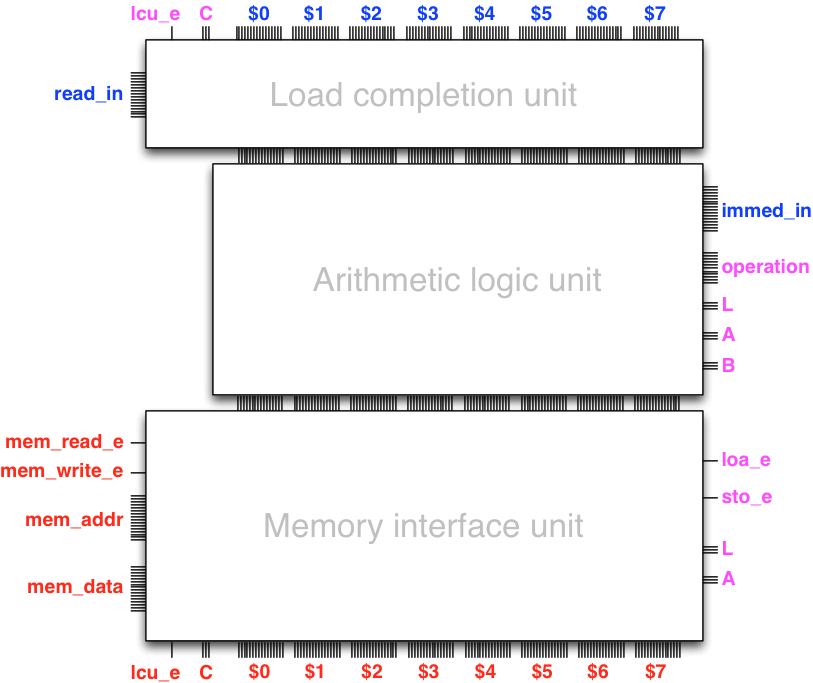
The data path has an interface to the memory unit (the outputs depicted on the left) and internal control feedback from the memory interface unit to the load completion unit (bottom-left outputs to top-left inputs). The data path is controlled by control inputs (inputs depicted on the right) that configure the arithmetic logic unit and the memory interface unit.
All in all, we observe that the data path is a rather versatile
machine that can maintain a state (both in its registers and in
a memory unit outside the processor proper) and evolve that state,
one operation at a time. Yet, recalling our Trigger time with
the ALU, we observe that it is rather cumbersome to configure
the control inputs to effect a particular operation. This is an
issue that needs our attention as designers, which is what we
proceed to do next.